


Electron Backscatter Diffraction (EBSD) Analysis
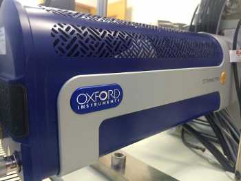
Oxford Symmetry electron backscatter diffraction detector
Microtrace offers electron backscatter diffraction (EBSD) testing services. EBSD analysis provides crystallographic and microstructural data about samples. This data can help identify phase, grain size, and crystal structure. Because of this, laboratories have typically applied EBSD testing to industrial or metallurgical samples. In Microtrace’s lab, our experts have developed and exploited many further applications for EBSD including forensic paint analysis and geosourcing of soils.
EBSD Analysis
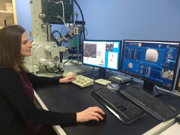
Microtrace’s FE-SEM with EBSD detector attachment.
Our EBSD system supplements the field emission scanning electron microscope (FE-SEM). In the EBSD process, the SEM’s electron beam interacts with a crystalline sample. The diffracted electrons produce a unique pattern. This “diffraction pattern” is characteristic of the crystal structure and orientation of the sample at the location of the beam. EBSD data can supplement EDS (Energy Dispersive X-Ray Spectroscopy) data to identify a crystalline phase, discriminate between polymorphs, or identify the orientation of a crystal. When we collect a matrix of EBSD data, our experts can map each pixel to reveal further information. We can use this data to determine the orientation of multiple grains relative to each other, discriminate between crystallographically different phases, study grain boundaries, and provide information about local crystalline perfection.
Microtrace’s laboratory utilizes the Oxford Symmetry detector:
- Image sensor: High-speed, low-noise CMOS, customised for EBSD
- Image size: 1244 x 1024 pixels (max.)
- Optics: Custom design, high efficiency, high-sharpness
- Distortion: < 1 pixel
EBSD Testing Services
Electron backscatter diffraction enables our lab to provide sample analysis beyond traditional SEM/EDS services. These analysis services include phase identification and mapping, and crystal identification and mapping. Our scientists have the expertise and experience to use EBSD for the analysis of polished or unpolished sections, single grains, or even nanomaterials.
Phase Identification from Grains
Our scientists can obtain diffraction patterns (EBSPs) from individual grain mounts. The SEM chamber accepts a sample at a highly inclined angle- typically, 70° to the normal. As an electron beam focuses on the sample, backscattered electrons reflect off of the lattice planes of the crystal. These reflected electrons form the EBSPs on a phosphor screen. From this image, the Oxford AZtec algorithm computes angles, slopes, widths, symmetries, and intensities of these EBSP bands. Finally, our experts compare this data to a reference database in order to identify the sample’s phase.
As an example, consider the EBSP of a polished silicon sample (see left image below). Note the pattern of intersecting bands that make up the EBSP. The algorithm detects these bands and compares the pattern to an indexed database. Our experts can then evaluate all possible solutions for the phase identification, based upon our expertise and knowledge of the sample. The image on the right superimposes a reference EBSP of silicon (yellow lines) over the sample’s EBSP. Our laboratory’s databases include: the Inorganic Crystal Structure Database (ICSD), American Mineralogist, Crystallography open database, HKL Phases, and OINA Phases.
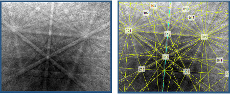
Figure 1: EBSP of silicon (left), and a reference EBSP of silicon superimposed (right).
Analysis by SEM/EDS and EBSD allow our experts to identify simultaneously the elemental composition of a sample and its crystallographic phase. This provides numerous analytical benefits to our laboratory. Often, sample size is limited and particles of interest are too small to resolve by light microscopy. The addition of this EBSD system to our lab allows us to view materials in high resolution, collect elemental data, and identify crystals within a single instrument.
EBSD testing of non-planar (unpolished) samples or individual grain mounts generally produces noisier and less pristine EBSPs. However, careful analysis can still lead to a successful phase identification (see images below). This method is useful for our soil and dust analysis services.
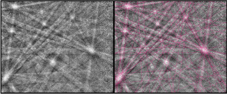
Figure 2. EBSP of an unpolished grain of quartz (left), and a reference EBSP of alpha quartz superimposed (right).
Crystal Orientation
When our experts use EBSD to pinpoint a sample’s phase, they also identify its crystal orientation. Our databases contain a model spherical reference (Kikuchi) projection for each phase in the collection. The Oxford algorithm compares the bands (reflectors) of these Kikuchi projections in every possible orientation against the sample’s 2-dimensional EBSP. Thus, any match is a match of both phase and crystal orientation, including the location and orientation of the crystal lattice and axes. Both are simultaneously identified. For example, the orientation of the 3D Kikuchi projection below matches the EBSP of polished silicon above. Note the blue highlighted reflector corresponds exactly with the blue diffraction band in the EBSP. The model also shows the crystal’s Miller indices (which describe the crystal faces), unit cell, and crystallographic axes.
Figure 3. Kikuchi projection of silicon oriented to produce the EBSP in Figure 1
In addition, Microtrace uses CrystalMaker software to help visualize crystal and molecular structures. This software allows us to create dynamic and rotatable modeled visualizations, which further enables us to design structures, predict certain properties, and explore interactions with other materials. In essence, EBSD is the high tech, electron microscopy version of the spindle stage, which utilizes polarized light microscopy and crystal optics to determine crystal orientation from a specimen mounted on a rotatable needle.
Phase Maps
Microtrace’s EBSD system and its accompanying AZtec software allows us to create maps. This feature automates the pixel-by-pixel collection of EBSPs, elemental compositions, and the resultant phase identifications of large areas of a specimen. The CMOS camera and lightning-fast SSD microprocessor allow for the rapid assemblage of the large amounts of data generated by this method. Accordingly, phase maps of the areas of interest within a sample can be created in order to analyze and characterize the relationships between adjoining crystal phases.
The phase map shown below is that of a polished steel specimen. This steel contains two crystal phases: body-centered cubic (BCC) steel, and face-centered cubic (FCC) steel, which are indicated in red and blue, respectively.
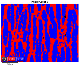
Figure 4. Phase map of a polished steel sample
Phase maps may also be created to study the distributions of sample components. A polished cross section of a paint containing lead carbonate (cerussite), barium sulfate (barite), zinc oxide (zincite), and talc mulled together with linseed oil is shown in Figure 5 below. Note the various colors representing the phases identified in the paint.
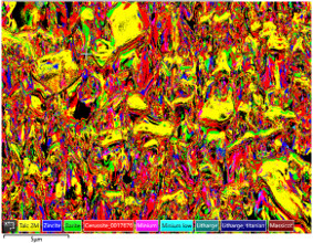
Figure 5. Phase map of a paint sample
Orientation Maps
Similar to phase maps, orientation maps can be constructed based on the EBSP patterns that illustrate the orientation of individual grains within a single phase. The grain structure, size, texture, and boundaries between grains help to characterize a specimen, and may indicate its method of formation, allow for sample comparison, or provide insights during failure analysis. The orientation map shown below displays the same area of the polished steel sample as the phase map depicted above; however, here the different colors represent grains in various orientations. Data analysis may be performed on the image to examine statistical data such as grain area, aspect ratio, and slope (of the grain’s major axis). The associated histograms can also be generated.
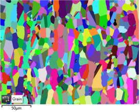
Figure 6. Grain orientation map of the steel sample from Figure 4
Transmission Kikuchi Diffraction (TKD)
The EBSD system has the added capability of collecting diffraction patterns from samples that are only a few nanometers thick, and are therefore transparent to electrons. This method, known as Transmission Kikuchi Diffraction (TKD), differs from traditional EBSD not only in the requirement that the sample be very thin, but also has an increased special resolution approaching that of a TEM. This is particularly useful for the characterization of nanostructures and nanomaterials, including ultra-fine grained steels and alloys, corrosion interfaces, and semiconductors.
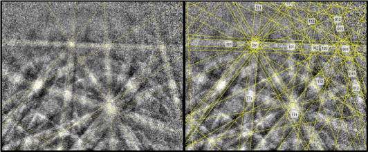
Figure 7. EBSP collected using TKD with a pigment-sized (200 nm) grain of TiO2 (left). A reference EBSP of the TiO2 polymorph anatase is superimposed on the image at right.
Sample Preparation for EBSD Testing
Sample preparation for electron backscatter diffraction is a critical step in obtaining good EBDPs. Ideal EBSD samples for testing are very flat, polished sections. However, our experts can obtain EBSPs from unpolished sections, individual grain mounts, or even nanomaterials.
Microtrace’s dedicated sample preparation laboratory includes ion beam cross section polishing, precision ion milling (Gatan 691 PIPS), and a vibratory polisher (Buehler). Our state-of-the-art lab allows our scientists to optimize client samples for EBSD testing.
EBSD Laboratory Submissions
Our experts conduct all services in our ISO 17025 accredited laboratory. We perform analyses in compliance with ASTM and ISO methods.
Our lab’s standard turn-around-time is 7-10 business days. However, rush (2-3 business days) and ultra-rush (same-day) options are also available.
EBSD analysis pricing is available upon request.
Contact us to learn how Microtrace can provide proper preparation and EBSD analysis of your samples.
EBSD Standardized Methods
ASTM (American Society for Testing and Materials) has created a standardized guide for EBSD analysis. E2627-13 “Standard Practice for Determining Average Grain Size Using Electron Backscatter Diffraction (EBSD) in Fully Recrystallized Polycrystalline Materials.”
ISO (International Organization for Standardization) also has a standardized guide for EBSD analysis. ISO 13067:2011 “Microbeam analysis — Electron backscatter diffraction — Measurement of average grain size.” This method is currently under review. ISO/DIS 13067 will replace this guide in the coming years.
How May We Help You?
Contact usto discuss your project in more detail.