


New Instrument- Electron Backscatter Diffraction (EBSD) System
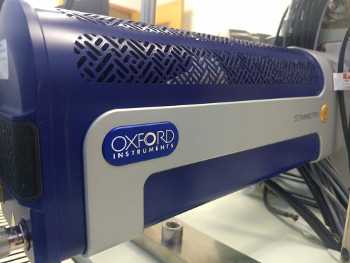
Microtrace recently added an electron backscatter diffraction (EBSD) system. Our Oxford Symmetry EBSD system is an accessory to the field emission scanning electron microscope (FE-SEM) that provides crystallographic and microstructural information. In the EBSD process, the electron beam from an SEM interacts with a crystalline sample to produce a pattern formed by diffracted electrons. The resulting diffraction pattern is characteristic of the crystal structure and orientation of the sample at the location of the beam. This data can supplement EDS data to identify a crystalline phase, discriminate between polymorphs, or identify the orientation of a crystal. When a matrix of EBSD data is collected, the resulting data at each pixel can be mapped to determine the orientation of multiple grains relative to each other, discriminate between crystallographically different phases, study grain boundaries, and provide information about local crystalline perfection. Although the technique has traditionally been applied to industrial or metallurgical samples, there are a number of potential applications to exploit, including forensic paint analysis and geosourcing of soils.
Microtrace utilizes the Oxford Symmetry detector:
- Image sensor: High-speed, low-noise CMOS, customised for EBSD
- Image size: 1244 x 1024 pixels (max.)
- Optics: Custom design, high efficiency, high-sharpness
- Distortion: < 1 pixel
For more applications of and information about this system, please see our EBSD page.
How May We Help You?
Contact usto discuss your project in more detail.